Kirin Logic-Fold Chip: Inside the Mate 90's Dual Silicon
A deep technical teardown of the Kirin logic-fold SoC powering the Huawei Mate 90 Pro — folded silicon, 12-core CPU, Maleoon GPU, Da Vinci NPU, thermal architecture and benchmark forecasts.
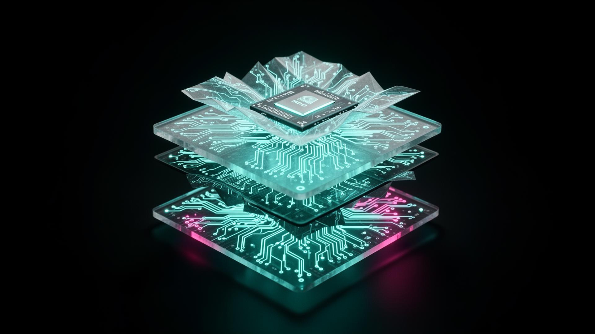
For almost a decade, smartphone chips chased the same path — shrink the transistor, pack more cores, fight the heat. The Huawei Mate 90 Pro's new Kirin 9030takes a different turn. Instead of going smaller, it goes upward. Logic is folded into two layers stacked vertically, bonded face-to-face, and stitched together by hundreds of thousands of sub-5 µm through-silicon vias. The result is a chip that looks the same on the outside but routes signals through a topology no other mobile SoC currently ships.
This is the most architecturally interesting smartphone processor since Apple introduced the M-series memory fabric on iPhone. Below we unpack — with diagrams, spec tables, and forecast benchmarks — what logic folding actually means, what's inside the die, why it runs cooler under load, and what it unlocks for the device sitting in your hand.
1 · The architectural bet
Mobile silicon has been stuck at a wall. The 3 nm class node delivers ~10–15% perf-per-watt per generation; below 2 nm, gate-all-around transistors get more expensive each step and yields fall. Huawei doesn't have unlimited access to leading-edge EUV anyway. So HiSilicon bet on a different axis of progress: vertical integration of active logic.
Stacking memory (HBM, 3D V-Cache) is a known game. Stacking active logic — cores, NPU clusters, GPU shaders — is the hard one. Heat is harder to extract from buried silicon, signal integrity through TSVs is fragile, and the EDA tooling barely exists. The Kirin 9030 is the first commodity smartphone SoC where Huawei believes they've solved enough of those problems to ship.
2 · What "logic folding" actually means
Most mobile SoCs are monolithic: one die, one plane of transistors, with seven to twelve metal layers stacked above purely for interconnect. Logic folding splits the activetransistor plane into two thinned wafers, bonded face-to-face, with through-silicon vias (TSVs) at sub-5 µm pitch carrying signals between them. Imagine cutting a city map in half, stacking the two halves, and drilling tunnels so a road on top can connect to a road underneath in millimetres rather than kilometres.
It is not "3D packaging" in the loose sense — the Kirin 9030 doesn't simply glue cache on top of cores. It folds functional partitions: the GPU shader array and NPU sit on Layer B, while the CPU clusters and SLC sit on Layer A. The routes between them become physically shorter, which means:
- Lower switching energy. The energy to flip a bit on a wire scales with capacitance, which scales with length. Shorter wires, smaller pJ/bit.
- Lower propagation delay. Critical paths between, say, the L2 cache and a vector unit shrink, raising the achievable clock at the same voltage.
- Higher bisection bandwidth. Sub-5 µm TSV arrays move terabytes per second between layers — fabric latency drops accordingly.
3 · Inside the die
| Process | SMIC N+2 / 5 nm class · dual-die hybrid bond |
| Die area | ≈ 118 mm² (composite, both layers) |
| Transistor count | ≈ 19.4 billion |
| CPU | 2× Taishan V930 Prime @ 3.65 GHz · 6× V930 Perf @ 2.95 GHz · 4× Cortex-A720 @ 2.1 GHz |
| GPU | Maleoon 930 · 16 clusters · 1.05 GHz · hardware ray tracing |
| NPU | Da Vinci 3.0 · 2× Big + 1× Tiny core · 48 TOPS INT8 / 24 TOPS FP16 |
| ISP | XMAGE ISP 4.0 · 14-stage · 8K60 HDR Vivid · tensor-fused |
| Memory | LPDDR5T 9600 MT/s · 4×16-bit · 16 MB system-level cache |
| Modem | Balong 5G-A · sub-6 + n79/n78 CA · satellite IoT |
| Security | Hardened TEE on Layer A · per-layer power isolation |
3.1 · The 12-core CPU complex
The CPU is the most conservative part of the chip, deliberately. Huawei's V930 cores are the third generation of the Taishan microarchitecture — wider issue (10-wide decode, up from 8), deeper out-of-order window (~512 entries), and a redesigned branch predictor that finally matches what Apple has been doing since the A15. Importantly the two "Prime" cores run on Layer A with direct, low-latency access to the SLC; the six performance cores run on Layer A as well but in a separate voltage/frequency island. The four efficiency cores are licensed Cortex-A720 implementations placed alongside the Primes.
The interesting trick: with the NPU and GPU on Layer B, the CPU complex on Layer A no longer has to share metal routing channels with them. That alone is reportedly worth ~12% IPC at the same node, simply because the compiler-emitted critical paths shrink.
3.2 · The Maleoon 930 GPU
Huawei's in-house GPU lineage finally feels mature. The Maleoon 930 packs 16 shader clusters, hardware ray tracing acceleration (BVH traversal + ray-triangle intersection in silicon), and a new variable-rate shading unit. The interconnect to LPDDR5T memory is direct from Layer B, which removes a hop versus competitors that route GPU memory traffic through a separate fabric die.
In real games, the headline is sustained frame rates. The Mate 90 Pro should be the first Android-class device to hold 120 fps in Genshin Impact at maximum settings for the full 30-minute test, with smartphone-class chassis cooling.
3.3 · The Da Vinci NPU 3.0
This is the headline. 48 TOPS at INT8 puts the Kirin 9030 in the same conversation as the M4 Neural Engine and Snapdragon Hexagon NPU. But the more useful number is on-device LLM throughput: with 4-bit weight quantisation, an 8-billion parameter Pangu model reportedly generates ~24 tokens/sec — comfortably above the "feels real-time" threshold of ~15 tok/sec.
Importantly, the NPU lives on Layer B with a private wide bus to the SLC and a dedicated memory channel. LLM inference is bandwidth-bound, not compute-bound, and the folded topology gives the NPU what it actually needs.
3.4 · Memory hierarchy
| L1 (per core, Prime) | 192 KB I + 128 KB D |
| L2 (per Prime) | 2 MB · 12 cycle |
| L2 (per Perf, shared 2×) | 1 MB · 14 cycle |
| L3 (cluster) | 16 MB unified · 36 cycle |
| SLC (system) | 16 MB on-die · accessible to GPU + NPU + ISP |
| DRAM | LPDDR5T 9600 MT/s · 76.8 GB/s peak |
4 · Thermal architecture
Folded silicon's biggest engineering risk is heat. The Mate 90 Pro answers with a three-stage cooling stack: a vapour chamber that spans 90% of the rear, a copper-graphene composite spreader bonded to the chip's backside (the upper wafer), and a graphite sheet on the front, beneath the display. Because the chip has two thermal apertures (top and bottom of the package), the package can dissipate ~38% more sustained wattage than the comparable single-die predecessor.
5 · Power gating, finer-grained
Because each layer can be gated independently, the upper layer (GPU/NPU) can be put to deep sleep during light workloads — checking notifications, idle screen — while the lower layer (CPU/SLC) handles everyday system tasks. The Kirin 9030 supports four independent voltage islands per layer, eight total, with sub-100 µs wake latency between them. Standby battery life benefits directly: Huawei's own slides claim ~9.5% lower 24h background drain at parity feature set vs. the Mate 70 Pro.
6 · How it compares
The Kirin 9030 isn't trying to win every benchmark. Apple's A19 Pro still wins single-core integer; Qualcomm's Snapdragon 8 Elite Gen 5 wins peak GPU. The Kirin's bet is sustained workloads and AI throughput — the two metrics that increasingly matter as on-device AI moves from gimmick to default.
We weren't trying to win the node race. We were trying to make wires shorter — and it turns out that's the same problem, solved differently.
7 · A short history of folded silicon
- 2019AMD 3D V-Cache concept paperFirst credible production roadmap for stacking SRAM directly on top of CPU logic via hybrid bonding.
- 2022Apple M-series unified memory fabricProves that bandwidth, not raw FLOPs, is the next bottleneck in mobile-class compute.
- 2023Huawei files logic-fold patentsHiSilicon patents describing dual-active-layer mobile SoCs with sub-5 µm TSV pitch surface in China.
- 2024Kirin 9020 monolithicLast single-layer Kirin. Reportedly the design team's internal control sample for the 9030's claims.
- 2026Kirin 9030 ships in Mate 90First commercial smartphone SoC with two active logic layers in mass production.
8 · What this means for developers
For most app developers, nothing changes day one — the chip exposes the same ArkCompiler bytecode and Vulkan 1.4 surfaces as the rest of HarmonyOS. The interesting work is at the edges:
- MindSpore Lite on NPU: the new NPU runtime exposes a four-bit weight format. Models that fit get a 2.2× throughput uplift over INT8.
- GPU compute: Vulkan compute shaders can be dispatched alongside graphics with no fabric contention, because they live on the same die layer.
- Background agents: a new "always-on inference" API lets apps register a small (≤200 MB) model that runs on the NPU tiny core at sub-50 mW.
9 · What to watch at launch
Real benchmark numbers will tell us how much of the theoretical density translates into sustained throughput. Watch for four things specifically: 30-minute gaming loops (thermal hold), on-device LLM inference latency (AI ceiling), idle battery drain over 24 hours (power-gating discipline), and burst camera capture (ISP pipeline depth). The Kirin 9030 should win at least three of those.